PCI Express SDR Board version 2026-07-03*This document is based on the latest test release.
Features may not be present in your current installed software. You may check their availability in change history or in your release documentation.
If you require an up to date release, ask for it in a ticket.
Features may not be present in your current installed software. You may check their availability in change history or in your release documentation.
If you require an up to date release, ask for it in a ticket.
Table of Contents
1 Features
- 2x2 RF transceiver (AD9361) with integrated 12-bit DACs and ADCs
- RF coverage: 500 MHz to 6.0 GHz
- RF bandwidth: < 200 kHz to 56 MHz
- Supports TDD and FDD operation
- Integrated TX/RX switch for TDD operation
- PCIe 1x standard connector
- Integrated GPS for precise time and frequency synchronization
- Clock/PPS inputs and outputs for easy chaining
- Optional sample compression to reduce the PCI bandwidth
2 Installation with the Amarisoft software
2.1 Introduction
If you have bought the OTS (Off-The-Shelve) package, then you donât need to install anything. Everything has already been installed on your PC. Otherwise, please follow through the steps below.
Decompress the trx_sdr archive into a convenient directory specified by <trx_path>.
tar -xzf trx_sdr-linux-YYYY-MM-DD.tar.gz -C <trx_path>
You have two ways to install the TRX driver for the PCIe card:
- automatic
- manual
For both cases, the installation requires some specific packages to compile the kernel module. To do this, you need to be root. In Fedora and Cent OS, you need to install kernel-devel, make, gcc and elfutils-libelf-devel packages by running the following command:
dnf install kernel-devel-$(uname -r) make gcc elfutils-libelf-devel
For Ubuntu, use the following command:
apt-get install linux-headers-$(uname -r) build-essential
Note that you’ll need equivalent packages for other Linux distributions if you do not use Fedora, Ubuntu or Cent OS.
Once you have finished the installation, you need to initialize (See Driver initialization) and upgrade your driver (See Firmware upgrade). Please make sure to initialize the driver after each system boot if you have not activates an automatic lte service.
2.2 Automatic Installation
Automatic installation is only available on Fedora, Ubuntu and CentOS distributions. Use manual install for other distributions. To start your automatic install, use the following command where <path> is the path to the directory where you have already installed your LTE component (eNB or UE) and type should be set to enb or ue accordingly.
./install <path> <type>
Notes:
- the script would install some packages, so make sure you have root privileges when you run the script
- this install creates a symlink for the TRX driver so please do not remove this directory afterwards.
2.3 Manual Installation
To manually install the driver, let’s note <path> the directory where Amarisoft eNB or UE software is installed. Then:
- Compile kernel driver:
Go to the kernel/ directory under <trx_path> and start compilation:cd kernel make
- Place driver:
Just copy the compiled driver into <path> directorycd .. cp trx_sdr.so <path> cp libsdr.so <path>
- Config files:
Copy RF driver config file. Note that there are 2 separate config directories for eNB and UE called config.enb and config.ue under your <trx_path>. As a result, the <config_dir> should be set to config.enb or config.ue accordingly.cp -r <config_dir> <path>/config/sdr
Select frontend:
<path>/config/rf_select.sh sdr
2.4 Driver initialization
Each time you boot your system, you need to perform this initialization. Note that if you are using OTS install, this step is already done by the lte service.
cd kernel
./init.sh
2.5 Firmware upgrade
Perform the following command to upgrade your PCIe card:
./sdr_util upgrade
Notes:
- If you have several PCIe cards installed, this will upgrade all cards.
- If the firmware is already up to date, this command will end directly.
- When the upgrade is over, you need your system to be powered off for the changes to take effect (not only reset, real power off).
2.6 Multiple card installation
To make several cards work together, they must be time and frequency synchronized. For that purpose you need to plug the provided black cable between each card. Connect the internal OUT connector (J4 on Figure 7.2) on the first card to the IN connector on the second card (J3 on Figure 7.2, connectors are between RoHS compliant mark and Serial number sticker). Then do the same with OUT of second card and IN of third one, etc...
When you install several PCIe cards, the mapping between the PCI connectors and the Linux devices is not predictable (but it shouldn’t change after each boot). To identify the order please do the following:
./sdr_util -c 0 led 1
Then check inside PC on each board, one of them should have a led blinking. This is card 0 (/dev/sdr0).
Switch off the led:
./sdr_util -c 0 led 0
You can do the same for other cards:
./sdr_util -c <n> led 1
Where <n> is the index of the card.
To use all the cards, update eNB config file (config.cfg) using args parameter:
args: "dev0=/dev/sdrA,dev1=/dev/sdrB,..."
Note: this allow to change the order of the cards. For instance, if your card are from left to right have following indexes:
<1> <2> <0>
And you want first cell to be on left, second cell to be on middle and third on right, use the following:
args: "dev0=/dev/sdr1,dev1=/dev/sdr2,dev2=/dev/sdr0"
2.7 RX Channel Mapping
Commercial CPEs have different antenna configurations depending on the band used. As an exemple, Telit FN980 CPE has different TX antenna mapping in bands n41 and n78 as shown in the following table:
| Antenna port | TX |
|---|---|
| ANT0 | n41 diversity antenna |
| ANT1 | n78 main antenna |
| ANT2 | n41 main antenna and n78 diversity antenna |
| ANT3 | No TX |
Amarisoft SDR50 card has 2 RX ports: RX1 and RX2 but the main RX antenna is always considered to be RX1 by default. In case of multiple streams in UL, the RX ports are used consecutively. As an example in case of MIMO 2x2 in UL, RX1 and RX2 will be used. This static setting is not practical when testing multiple bands in conducted mode. Let’s consider a cabled test with the Telit CPE FN980. In case of n78, the CPE ANT1 should be connected to the RX1 port of the SDR card while in n41, the CPE ANT2 should be connected to RX1.
In order to make the cabling easier, we have introduced a new parameter in the RF driver called rx_chan_mapping(See rx_chan_mapping) which defines the list of physical RX ports to be used per RF port. This parameter is a string separated by , for each RF port. Inside each RF port, there is a list of physical RX port indexes that are used by each UL stream.
|
|
Let’s take an example of a configuration with one cell MIMO 4x4 in DL and SISO in UL in n78 connected by cables to a Telit FN980 CPE with 4 antenna ports as depicted below.
This configuration can be run on two SDR50 boards.
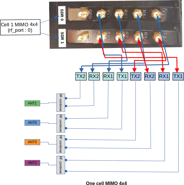
The CPE uses ANT1 as the main antenna for UL in band 78. However, the ANT1 is connected physically to TX2/RX2 as can be seen in the above figure. Setting rx_chan_mapping to 1 means that the SDR driver should expect to receive the UL data on the RX2 port (the index of RX2 is one). The corresponding rf_driver configuration is as below. There is only one single stream in UL which is mapped to RX2 and there is only one cell (one rf_port) in this example.
rf_driver: {
        name: "sdr",

        /* list of devices. 'dev0' is always the master. */
        args: "dev0=/dev/sdr0,dev1=/dev/sdr1",

        /* TDD: force the RX antenna on the RX connector */
        rx_antenna: "rx",

        /* synchronisation source: none, internal, gps, external (default = none) */
        // sync: "gps",

        rx_chan_mapping: "1",
}
Now, let’s consider another example with 2 cells MIMO 2x2 in DL and SISO in UL. This configuration can be run on two SDR50 boards as depicted below.
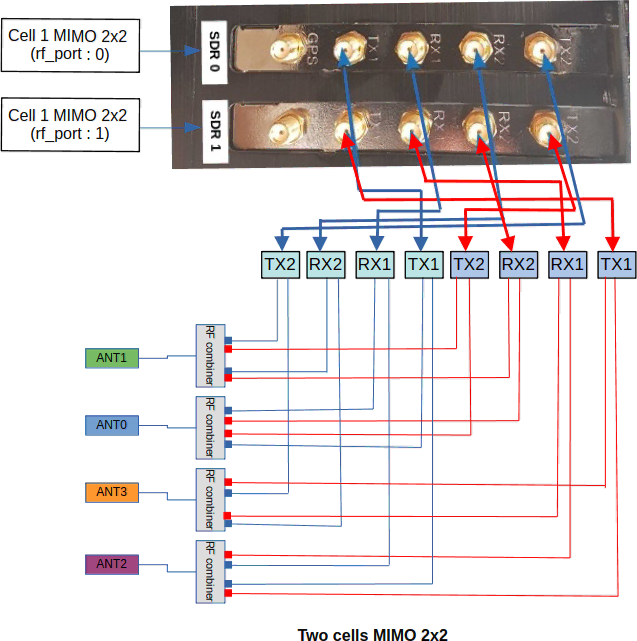
The first cell (rf_port 0) is in n78 and the second one is in n41. Let’s consider again that a TELIT CPE is used where the UL main antenna is ANT1 in case of n78 and ANT2 in case of n41. There is still one single layer in UL. In this case, rx_chan_mapping should include 2 indexes, one for each RF port. The first index refers to the RX port used to receive the UL in rf_port 0 (Cell 1 in n78) while the second one is the RX port index in rf_port 1 (Cell 2 is n41).
The following rx_chan_mapping means that the UL stream is expected to be received on the RX2 port of the first board and the RX1 port of the second board.
rx_chan_mapping: "1,0",
Now let’s consider the same example as above with 2 cells but this time UL is in MIMO 2x2 in both cells. Remember that Telit CPE uses ANT1 and ANT2 as main and diversity antenna for n78 and ANT2 and ANT0 as main and diversity antenna for n41. With respect to the cabling of the above diagram, the rx_chan_mapping should be as follows.
rx_chan_mapping: "1:0,0:1",
In the rf_port 0 (n78 Cell), the RX2 and RX1 ports are used to receive the UL stream 0 and stream 1 while in the rf_port 1 (n41 cell), the RX1 and RX2 ports are used.
2.8 TDD support
The board integrates a TX/RX switch for TDD operation. When TDD operation is configured, the transmit and receive are done on a single RF port (the TX SMA connector). So you only need to connect antennas on the TX1 and TX2 SMA connectors for TDD operation.
2.9 GPS usage
You can check the GPS operation when the eNodeB/UE is stopped with
./sdr_util gps_state
The GPS takes a few minutes to lock if the GPS antenna is
connected. Any active GPS antenna accepting a 3.3V DC supply can be
used, for example: http://www.mouser.fr/Search/ProductDetail.aspx?R=ANT-GPS-SH-SMAvirtualkey59000000virtualkey712-ANT-GPS-SH-SMA
To ensure the PLL is correctly locked when launching the lte software, it is recommended to set the synchro to GPS beforehand with the command
./sdr_util sync_gps
2.10 Oscillator frequency fine tuning
If you don’t have a GPS, it is still possible to manually fine tune the VCTCXO (Voltage Controlled, Temperature Controlled Crystal Oscillator) frequency provided you have a way to know the offset:
./sdr_util clock_tune n
where n is the offset in PPM (parts-per-million) from the nominal TCXO frequency. Note: the PPM offset n to voltage law is only approximative, so you should adjust it by successive approximation.
3 TRX driver configuration options
3.1 Single card configuration
The following properties are available:
namerf_driver.nameString. Set the driver to use, always set "sdr" to use Amarisoft driver.
argsrf_driver.argsString. Set the system device names for the boards. Example:
args: "dev0=/dev/sdr0"
args: "dev0=/dev/sdr0,dev1=/dev/sdr2"
sample_hw_fmtrf_driver.sample_hw_fmtOptional enumeration (auto, ci16, cf8) (default = auto). Set the sample format used on the PCI bus.
autoselects the best format depending on the available PCI bandwidth.ci16selects 16 bit complex integers.cf8selects 8 bit complex floats giving a 2:1 compression ratio while retaining the full 12 bit amplitude of the ADCs and DACs.rx_antennarf_driver.rx_antennaOptional enumeration (auto, tx_rx, rx) (default = auto). Select the connector on which the RX antenna is connected. By default it is connected on the RX connector for FDD and on the TX/RX connector for TDD. This parameter is useful to force the use of the RX connector in TDD.
fifo_tx_timerf_driver.fifo_tx_timeOptional number. Set the DMA TX buffer size in us.
Decreasing this value will improve latency but may lead to signal samples loss if the PCIe chain on the motherboard is not fast enough. This can be detected with therf_infomonitor command of yourlteenborlteuesoftware. If such situation happens, the percentage ofTX buffer Usagewill be 100% which means the transmission path has encountered underflows.fifo_rx_timerf_driver.fifo_rx_timeOptional number. Set the DMA RX buffer size in us.
Same asfifo_tx_timefor RX chain but reducing it won’t improve latency.pps_extra_delayrf_driver.pps_extra_delayOptional float value in microseconds, range: [-10000.0 .. +10000.0] (-10ms to +10ms) Adds a delay between GPS pulse and start of DL frame. If the pps_extra_delay value is negative, the actual delay will be (10ms + pps_extra_delay). For instance, if you want to compensate for 250ns delay caused by cable length, you will set pps_extra_delay: -0.25, the software will add (10ms - 250ns) to the GPS pulse.
tdd_tx_modrf_driver.tdd_tx_modOptional number value: 0 (default) or 1. If set to 1, the TX amplifiers will be switched on and off according to the TDD state.
rx_chan_mappingrf_driver.rx_chan_mappingOptional string. By default, if the radio frontend has more RX channels available than configured (ex: more physical RX connectors on SDR or more channels in CPRI hyperframes), the driver uses the first channels of the radio frontend.
This parameter allows to select the RX channels of the radio frontend to use.
This parameter is a list of number (must have as many number as RF port configuration) separated by colons. Each number represents the RX channel of the radio frontend to use.Ex: If a RF port has 4 TX antenna and 2 RX antenna, by default driver will use RX1 and RX2 of first SDR board. By setting:
1:2
RF driver will use RX2 of first board as primary RF port channel and RX1 of second board as secondary RF port channel.
With:
3:1
RF driver will use RX2 of second board as primary RF port channel and RX2 of second board as secondary RF port channel.
syncrf_driver.syncOptional enumeration: none, internal, gps, external (default = none).
Set the time synchronization source (Pulse Per Second).
noneandinternaluses the internal PPS generated from the clock.
internalsynchronizes the RX timestamps on the internal PPS.
nonedoes not synchronize the RX timestamps on the internal PPS for a faster startup.
gpsuses the internal GPS.
externaluses the PPS from the IN connector (J3 on Figure 7.2) if clock source is selected asexternalor from the PPS MMCX connector (PR10) if clock source is selected asinternal.
When several cards are selected (with the
argsproperty),synconly sets the time synchronization source of the first card. The other cards are implicitly set toexternalsynchronization, assuming the previous card is used as source (except if sync_mode isseparate).
clockrf_driver.clockOptional enumeration: internal, external (default = internal).
Set the clock source.
internaluses the internal clock (VCTCXO). If an external PPS sync source is used, the internal clock frequency is adjusted by the PPS signal.
externaluses the clock from the IN connector (J3 on Figure 7.2).
When several cards are selected (with the
argsproperty),clockonly sets the clock source of the first card. The other cards are implicitly set toexternalclock, assuming the previous card is used as source (except if sync_mode isseparate).
sync_moderf_driver.sync_modeOptional enumeration: cable (default), pcie, separate.
Select the inter board synchronization mode.
cableuses the standard cable between boards (IN / OUT connectors).
pcieuses the PCIe bus itself instead of cables.
Remark: it takes a few dozen extra seconds at launch time. It also allows syncing between SDR50 and SDR100.
separatemeans each board uses its own independant sync and clock.
gpio0rf_driver.gpio0Optional enumeration. Selects the signal ouput on test point TP3. See below for possible values. Default = rf_dts1.
gpio1rf_driver.gpio1Optional enumeration. Selects the signal ouput on test point TP4. See below for possible values. Default = rf_dts2.
gpio values:Value Description zero output a constant low level signal (OV) one output a constant high level signal (3.3V) rf_dts1 in TDD mode, output a high level when the TX is active on channel 1. Polarity can be inverted by setting dts_polarity: lowrf_dts2 in TDD mode, output a high level when the TX is active on channel 2 Polarity can be inverted by setting dts_polarity: lowpps_selected output a positive going Pulse per Second from the currently selected sync pps_ext output a positive going Pulse per Second from the EXT PPS MMCX onboard connector pps_prev output a positive going Pulse per Second from the IN 5 pin inter board connector pps_gps output a positive going Pulse per Second from the onboard GPS module pps_vcxo output a positive going Pulse per Second from the onboard generator dma_tx output a positive front on each TX DMA packet (synced on current selected PPS) dma_rx output a positive front on each RX DMA packet dma_tx_100Hz output a 100 Hz signal synced with dma_tx dma_rx_100Hz output a 100 Hz signal synced with dma_rx dts_polarityrf_driver.dts_polarityOptional enumeration: high (default), low. Selects the polarity for both rf_dts1 and rf_dts2 signals.
The range for the transmit gain (tx_gain parameter in
eNodeB/UE) is from 0 to 89.75 dB. The range for the receive gain
(rx_gain parameter in eNodeB/UE) depends on the frequency:
| Frequency | Gain |
|---|---|
| 70-4000 MHz | 3 to 71 dB |
| 4001-6000 MHz | 0 to 62 dB |
The maximum sample rate is 61.44 MHz.
3.2 Multiple card configuration
All single card configuration parameters apply to multiple card mode.
To differentiate configuration for each card, the syntax of some parameter will change
to a list of value separated by commas (,).*
The first value will apply to the first board defined in args argument, ...
This syntax applies to the following parameters:
- pps_extra_delay
- fifo_rx_time
- fifo_rx_ratio
- fifo_tx_time
- fifo_tx_ratio
- rx_chan_mapping
4 Troubleshooting
Below are a few tips on how to handle different errors.
- The eNodeB does not start and the output of
dmesglinux command resembles the following error message:
sdr: version magic '4.12.9-200.fc25.x86_64 SMP mod_unload' should be '4.12.11-200.fc25.x86_64 SMP mod_unload'To resolve it, you need to recompile the SDR driver on the PC (See Manual Installation).
5 Miscellaneous utilities
5.1 sdr_util
usage: sdr_util [options] cmd [args...]

Options:
-h                         help
-c device_num              select the device (default = all)

Available commands:
version                    dump the FPGA version
sync_state                 dump the synchro and clock state
gps_state                  dump the GPS state
sync_gps                   select GPS as sync source, wait for stable state
gps_cal [-s]               uses the GPS sync to tune VCXO, optionnaly stores
                           the value in flash
temp                       dump the temperature of the board components
led [0|1]                  enable/disable led blinking
clock_tune n               tune TCXO frequency offset to n ppm
upgrade [options]          upgrade the FPGA firmware
  upgrade options are:
  -force                   force upgrade even if identical or
                           previous version
5.2 sdr_spectrum
sdr_spectrum is a real time spectrum analyzer, sample viewer
and I/Q file recorder. It handles several channels at the same
time. It can be invoked without arguments. The following options are
available:
-hhelp
-args strset the device arguments (default="dev0=/dev/sdr0")
-rx_freq freqset the RX frequency in Hz (default=2400000000)
-rate rateset the sample rate to ’rate’ Hz (default=30720000)
-rx_gain gainset the RX gain in dB (default=60)
-channels cset the number of RX channels to ’c’ (default=1)
-rx_bwset the analog receive bandwidth in Hz (default=same as sample rate)
-sync sourceset the sync source to ’source’ (none, internal, gps, external) (default=none)
-clock sourceset the clock source to ’source’ (internal, external) (default=internal)
-save_path pathset the directory where the recorded samples are saved (default=/tmp)
-duration dset the recorded sample file duration in seconds when saving (default=1.0)
-savestarts recording samples automatically from program start.
-save-and-exitsame as
-savebut program will quit at end of recording.
When saving the recorded samples, one file is generated per channel. The filename contains the UTC date, the frequency and the channel number. The I/Q samples are saved as little endian 32 bit float values, in I/Q order. The sample values are between -1 and 1.
Invocation example:
./sdr_spectrum -channels 2 -rx_gain 50 -rx_freq 2680e6 -rate 30.72e6
Resulting output:
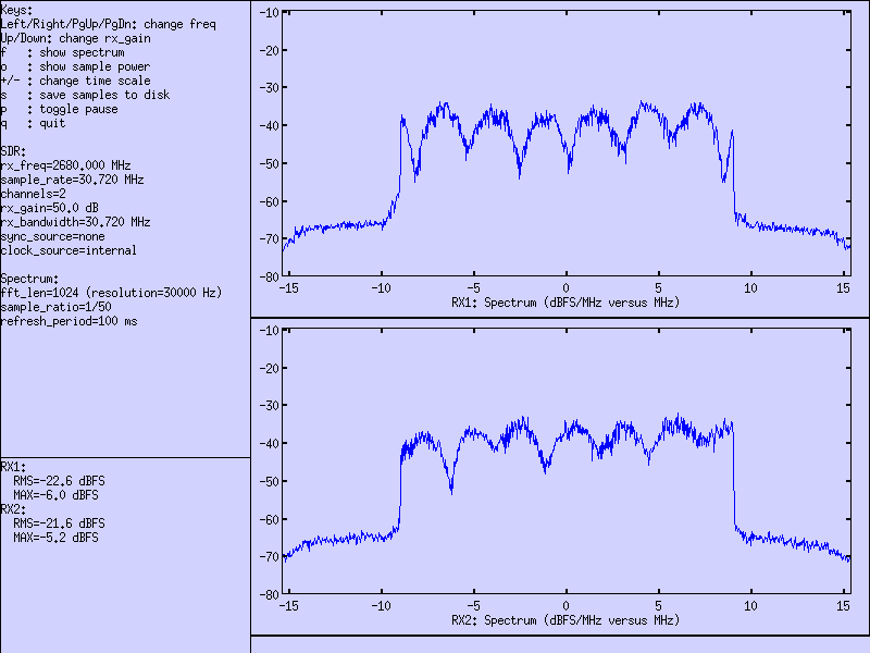
sdr_spectrum is interactive and allow actions during runtime:
keysavailable keys are indicated in the left side text area.
left mouse buttonselect a range and the X-Y values are displayed on the bottom of the graph.
right mouse buttonin spectrum mode, highlight a range and get a measure of the power inside the range.
5.3 sdr_play
sdr_play is an I/Q file player. Several channels can be played
at the same time and they can be time synchronized on an external
clock. One file must be provided per channel. The following options
are available:
-hhelp
-args strset the device arguments (default="dev0=/dev/sdr0")
-tx_freq freqset the TX frequency in Hz (default=2400000000)
-rate rateset the sample rate to ’rate’ Hz (default=23040000)
-tx_gain gainset the TX gain in dB (default=70)
-channels cset the number of channels to ’c’ (default=1)
-tx_bw bwset the analog transmit bandwidth in Hz (default=same as sample rate)
-loopplay the file in loop
-sync sourceset the sync source to ’source’ (none, internal, gps, external) (default=none)
-clock sourceset the clock source to ’source’ (internal, external) (default=internal)
-time_offset noffset the output by n samples (default=0)
The sample files should contain the I/Q values as little endian 32 bit floats, in I/Q order. The sample values should be between -1 and 1.
5.4 sdr_test
sdr_test is a general diagnostic tool for SDR boards.
usage: sdr_test [options] cmd [args...]
-hhelp
-c device_numselect the SDR device number (default=0)
-d channelselect the device channel (default = 0). useful for CPRI boards.
dma_loopback_test [n][sec]test DMA loopback on 1 or n devices for sec seconds (def: 10)
rfic_tx_test sample_rate freq tx_gain waveform [tone_freq/ofdm_bw]test RFIC TX (freq in Hz, tx_gain in dB from 0 to 90)
waveform can be:zero for no signal prbs for PRBS simulation, tone for CW at specified offset from center freq (default = 7.68e6) ofdm for OFDM simulation on specified bw (default = auto)
flash_checkverify checksum of code in onboard FPGA.
flash_reloadreload FPGA code from onboard flash
gps_readGPS read test (best with GPS antenna)
ledblinks onboard led during 5 seconds for identification
synchro_set [src]Set the source for PPS synchronisation
 0=internal
 1=GPS
 2=slave
 3=ext PPS
 4=CPRI
 5=ext CLK
synchro_stateShow current status of clock and synchro source for SDR device
Example:
 sync_source = 0 (internal)
 pps_locked = 1
 clock_source = 0 (internal)
 clock_pll_locked = 1
versionShow SDR device Hardware and firmware information
Example:
 Board ID:         0x4b01
 Board master:     0x0
 Board revision:   0x0
 FPGA revision:    2022-06-07 16:29:58
 FPGA status:      operational
 Software version: 2022-02-25
dump_infodump fpga and RF chip information (similar to sdr_util version)
Example:
PCIe SDR TRX driver 2022-02-25
PCIe RFIC /dev/sdr0@0:
  Hardware ID: 0x4b01
  DNA: [0x107149909461141596]
  Serial: ''
  FPGA revision: 2023-06-27  15:31:17
  FPGA vccint: 1.00 V
  FPGA vccaux: 1.79 V
  FPGA vccbram: 1.00 V
  FPGA temperature: 42.6 °C
  AD9361 temperature: 18 °C
  AGC: Off
  Sync: internal (locked)
  Clock: internal (locked)
  Clock tune: -0.7 ppm
  NUMA: 0
  DMA: 1 ch, 64 bits, SMem index: On
  DMA0 TX_Underflows: 65535  RX_Overflows: 65535
  PCIe bus: bus=0xb4 FPGA PCI gen2 x1 (4.0Gb/s)   OK
gpio 0|1 [value]Get or set the signal available on GPIO points on the board
Seegpio0andgpio1in chapterTRX driver configuration options;
6 C API
The PCIe SDR board can be used in other projects with its C API. The C
API allows to send and receive I/Q samples and to change the various
parameters (frequency, sample rate, bandwidth, gains, ...). The
Amarisoft TRX driver, sdr_play and sdr_spectrum are
built using this API.
The C API is described in libsdr.h. The corresponding Linux x86_64 dynamic library is libsdr.so.
Amarisoft does not provide any support for this API and can modify it without notice.
7 Physical specifications
7.1 Summary
- RF power output < 10 dBm
- Max RF input power: ~ -10 dBm RMS (+2dBm peak)
- 4 SMA female (TX1, TX2, RX1, RX2), AC coupled
- 1 SMA female (GPS antenna with 3.3V DC power supply)
- 2 internal 5-pin connectors for inter-card time synchronization
- 1 internal MMCX connector for external PPS input
- PCIe gen2 x1, full height, short length
- Uses single 12V power supply from PCI connector
- ADC/DAC Sample Rate: maximum 61.44 MS/s
- ADC/DAC Resolution: 12 bits
- Frequency Accuracy: 2 ppm
- LTE 20MHz 64QAM EVM < 2 %rms (f < 2.6 GHz)
- LTE 20MHz 64QAM EVM < 4 %rms (f < 3.5 GHz)
- Full size (L x W x H): 128mm x 115mm x 20mm
- Weight: 0.100 kg
- Power (PCIe 12V): 210mA idle => 2.5W, 460mA maximum (2x2 max tx_gain) => 5.5W
7.2 Connectors
The following figure depicts the location and functionality of each connector in the PCIe board.
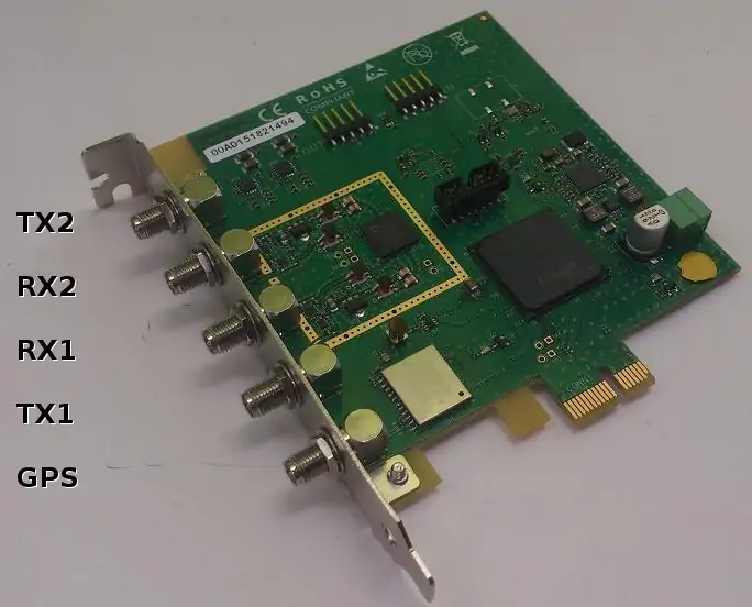
Figure 7.1
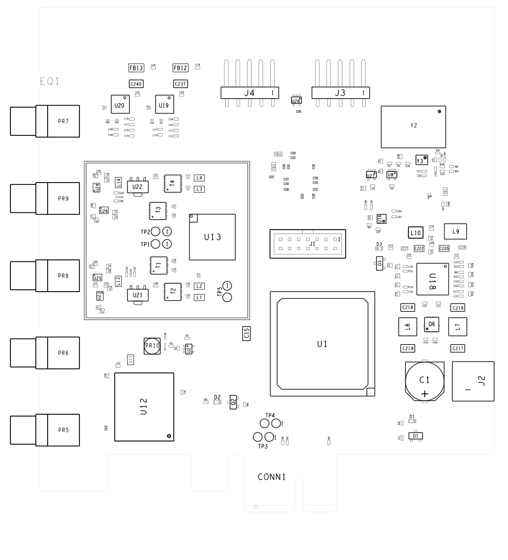
Figure 7.2
7.2.1 SMA connectors
See Figure 7.1 for the location.
On Figure 7.2, the connector names are:
PR7TX2 (and RX2 for TDD)
PR9RX2 (for FDD)
PR8RX1 (for FDD)
PR6TX1 (and RX1 for TDD)
PR5GPS
7.2.2 PPS/Clock connectors
OUT connector (J4):
1PPS_OUT
2REFCLK_OUT_N
3REFCLK_OUT_P
4,5GND
PPS_OUT is a LVCMOS 3.3V output.
REFCLK_OUT is a LVCMOS 2.5V signal with AC coupling.
IN connector (J3):
1PPS_IN
2REFCLK_IN_N
3REFCLK_IN_P
4,5GND
PPS_IN is a LVCMOS 3.3V input (> 3.3V input is not accepted).
REFCLK_IN is a LVCMOS 2.5V signal with 100 ohm impedance and 1.2V center voltage.
This reference clock is 38.4 MHz when used to synchonize between SDR boards.
It can also accept a 10.0 MHz reference clock (auto detect).
5 or 4 pin USB2 motherboard PC cables can be plugged in J3 and J4.
When using a 4 pin connector, pin 5 can be left unconnected.
7.2.3 PPS MMCX connector
- PR10
MMCX input connector for external PPS source
- Imped.
50 ohms.
- Level
CMOS, positive pulse.
7.2.4 JTAG connector (J1)
JTAG connector:
1,3,5,7,9,11,13GND
2VCC (3.3V)
4JTAG_TMS
6JTAG_TCK
8JTAG_TDO
10JTAG_TDI
12,14NC
7.2.5 Test Pins for TDD mode
See Figure 7.2 for the location. These pins are 3V3 CMOS output, they are driven high when RF port is in TX mode. They can be used to signal external RF circuitry in TDD mode.
TP3see
gpio0option in chapterTRX driver configuration options; default value = rf_dts1 (TDD switch for TX1 port)TP4see
gpio1option in chapterTRX driver configuration options; default value = rf_dts2 (TDD switch for TX2 port)
7.3 RX power
Maximum RX power on any RX port to avoid damage: -10dBm RMS.
7.4 TX power
Maximum RMS TX Power versus RF frequency, measured on OFDM bandwidth = 20MHz and tx_gain = 90.
Also Peak dBm tone power, about 12dB higher due to average peak/RMS ratio.
Both were measured using sdr_test rfic_tx_test with ofdm and tone options.
(sdr_test version dated after November 2024 needed for actual maximum range).
Actual power reached may vary by a few dBm because of hardware variations.
| RF Frequency (MHz) | OFDM (dBm/MHz) | OFDM (dBm) | Tone (dBm) |
|---|---|---|---|
| 500 | -10.0 | 3.0 | 14.5 |
| 1000 | -10.0 | 3.0 | 14.5 |
| 1500 | -14.0 | -1.0 | 12.0 |
| 2000 | -15.0 | -2.0 | 10.0 |
| 2500 | -15.5 | -2.5 | 10.0 |
| 3000 | -17.5 | -4.5 | 7.5 |
| 3500 | -17.5 | -4.5 | 7.5 |
| 4000 | -18.5 | -5.5 | 6.5 |
| 4500 | -22.0 | -9.0 | 2.0 |
| 5000 | -27.5 | -14.5 | 0.0 |
| 5500 | -31.0 | -18.0 | -4.0 |
| 6000 | -31.0 | -18.0 | -4.0 |
8 Remote API
SDR driver implements the trx remote API.
Message definition:
commandtrx.commandOptional string. Can be:
- clock_tune
Exemple:
{
    "message": "trx",
    "command": "clock_tune"
}
Here are the additional request and response field depending on command value:
8.1 clock_tune
Request fields:
offsetOptional number. If
commandisclock_tune, defines the clock drift to set in ppm.
9 Change history
9.1 Version 2026-07-03
- Added
pciemultiple card synchronization mode
9.2 Version 2026-06-12
- Added
sdr_spectrumforaarch64
9.3 Version 2025-12-12
- Added 16 bits float support for TRX driver
9.4 Version 2025-06-13
- Added
rx_chan_mappingconfiguration parameter
9.5 Version 2024-06-14
- Added remote API support
9.6 Version 2023-09-08
- Added NUMA support
9.7 Version 2023-06-10
- Added tdd_tx_mod configuration parameter
- New FPGA firmmware version 2023-05-24
10 License
trx_sdr is copyright (C) 2012-2026 Amarisoft. Its redistribution
without authorization is prohibited.
trx_sdr is available without any express or implied warranty. In
no event will Amarisoft be held liable for any damages arising from
the use of this software.
For more information on licensing, please refer to license terms.